Eecs:1100 Digital Logic Design Final Examination Eith Answers - Dr. Anthony D. Johnson, The University Of Toledo Page 5
ADVERTISEMENT
 1
1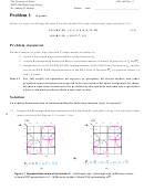 2
2 3
3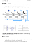 4
4 5
5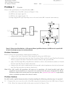 6
6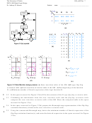 7
7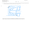 8
8The University of Toledo
f15fs_dild7.fm - 5
EECS:1100 Digital Logic Design
Dr. Anthony D. Johnson
Student
name
______________________________________
Hint #1 For full credit: all equations, all answers to questions, all circuit models and other
graphical representations are expected to be entered into the space designated for them;
all shown numerical results must be preceded by the
symbolic and numeric
expressions
whose evaluation produces the shown results.
Problem Solution
For full credit, explicit demonstration of understanding the following solution steps is expected.
2.1 Using for the input signals to the shift register the following designations:
8
- for the shift right operation: I
,
SR
- for the shift left operation: I
,
SL
- for parallel load operation: I
through I
o
3
design and enter in Figure 2.1(a) the necessary connections to make the completed circuit model
of Figure 2.1(a) implement the universal shift register specified by the function table shown in
Figure 2.1(b).
2.2 In the space reserved for Figure 2-1(c), write the signal designations from Figure 2.1(a) which
represent the serial outputs of the register for the shift left and shift right operations.
2
ADVERTISEMENT
0 votes
Related Articles
Related forms

 - The University Of Arizona")


Related Categories
Parent category: Education